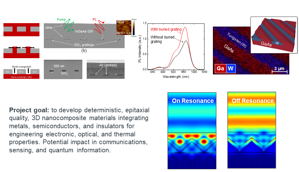
Growth of crystalline materials has yielded exquisite control of thickness in the vertical direction, nearing atomic layer precision across large diameter substrates; however, spatial control in the lateral direction lags dramatically with only middling control from self-assembled growth processes. By contrast, modern 3D printing with interference lithography has achieved subwavelength control in all dimensions down to 100 nm; unfortunately, the materials used are not suitable for active optical and electronic systems. The goal of the project is to bridge this dichotomy of capabilities to bring full 3D control of the growth of crystalline semiconductors and to begin to explore the unique electrical, optical, and thermal properties the resulting composite structures would afford. Such a synthesis platform would be enabling for industries ranging from communications to chemical/biological sensing.
Seth Bank | Electrical and Computer Engineering
Yaguo Wang | Mechanical Engineering
Daniel Wasserman | Electrical and Computer Engineering
Feng He | Mechanical Engineering
Ashlee Garcia | Electrical and Computer Engineering
Priyanka Petluru | Electrical and Computer Engineering
Alec Skipper | Electrical and Computer Engineering