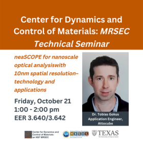
neaSCOPE for nanoscale optical analysis with 10nm spatial resolution – technology and applications
Every scientific question has its own merits and demands specific instrumentation to search for answers. Nanoscale IR is a new versatile technology which allows to probe material properties such as chemical composition, molecular orientation, stress & strain fields, and free-carrier concentration with 10 nm spatial resolution. It combines and exploits the benefits of two well established technologies, Atomic Force Microscopy (AFM) and Infrared microscopy and spectroscopy. An IR laser beam is focused on the apex of an AFM tip creating a nano-sized optical probe at the tip-sample interface. Acting as a local probe, the AFM tip senses the optical tip-sample interaction. By detecting either the light emitted from the area right below the tip (nano-FTIR) or by detection of the cantilever deflection and dynamics (tapping AFM-IR+) IR images and spectra with nanoscale spatial resolution can be obtained. Depending on the individual research needs, it is also possible to opt for VIS, IR or THz light sources and use a transmission mode instead of reflection. In our presentation, we shall explain the basic working principle of nanoscale infrared microscope modes available for the neaSCOPE and highlight the benefits by presenting application examples from a broad spectrum of materials such as polymers, minerals, 2D materials and semiconductors.
Biography
Dr. Tobias Gokus finished his Diploma at the University Siegen and Tübingen working on single molecule/particle optical microscopy and spectroscopy. For his PhD he joined the group of Prof. Achim Hartschuh at LMU, Munich for developing dedicated confocal and near-field optical microscopes optimized for studying the luminescence properties of low dimensional carbon materials. Captivated by the possibility to introduce the huge application potential of infrared near-field microscopy to a broader scientific community Tobias joined the nanoscale analytics department (ALX) of Attocube Systems AG as application engineer. In his current position he is exploring together with researchers in academia and industry new applications of near-field microscopy for their research.